
Delving into Photonic Integration Principles
In today's fast-paced world, the demand for faster and more efficient technology is on the rise. Enter photonic integration, a technology that combines the power of optics and electronics to create high-speed data transfer and efficient processing. In this section, we will explore the principles of photonic integration and gain a deeper understanding of the fundamental aspects of light technology and optics.
Key Takeaways
- Photonic integration combines optics and electronics to create high-speed data transfer and efficient processing.
- Understanding the principles of optics and light technology is essential for comprehending photonic integration.
- Photonic integration features various key components such as waveguides and modulators.
- Manufacturing processes such as lithography and etching are crucial in fabricating integrated photonic devices.
- Photonic integration offers various benefits such as enhanced performance and miniaturization of devices.
What is Photonic Integration?
Photonic Integration refers to the process of combining optical and electronic elements on a single microchip. It allows for the creation of complex optical systems, which can be integrated with electronic circuits to produce highly efficient devices with a range of applications.
At its core, photonic integration involves the use of various components, such as waveguides, modulators, and detectors, which are integrated with electronic circuits to create a fully functional photonic device.
The applications of photonic integration are vast and varied, ranging from telecommunications and data centers to medical devices and sensing technologies. In the following sections, we will explore the many applications and benefits of photonic integration in more detail.
The Basics of Optics
Optics is the branch of physics that describes the behavior and properties of light. Understanding optics is crucial to the development and application of photonic integration.
Light has unique properties that distinguish it from other types of energy. For example, it travels in straight lines, and its speed is constant in a vacuum.
Reflection and refraction are two fundamental principles that govern the behavior of light.
Reflection
Reflection is the phenomenon of light bouncing off a surface. The angle of incidence, which is the angle between the incident ray and the normal to the surface, is equal to the angle of reflection, which is the angle between the reflected ray and the same normal.
Many materials, such as metals and mirrors, have high reflectivity and are used to reflect light in various applications.
Refraction
Refraction is the bending of light as it passes from one medium to another. This bending is caused by the change in the speed of light as it moves from one medium to another.
The amount of bending depends on the angle at which the light enters the new medium, as well as the properties of the media involved. Refraction is responsible for a wide range of phenomena, from the way lenses focus light to the way rainbows are formed.
Light has many other properties that are important to photonic integration, including polarization, interference, and diffraction. A thorough understanding of optics is essential to the development and application of integrated photonic devices.
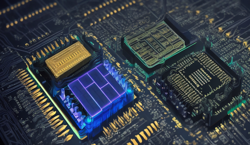
Components of Photonic Integration
Photonic integration involves combining optics and electronics to create high-performance devices that enable faster data transfer and processing. This process involves several key components, including waveguides, modulators, and other essential elements.
Waveguides
Waveguides are one of the fundamental components of photonic integration. They are optical structures that guide light waves through a medium, such as a semiconductor or polymer. Waveguides come in several forms, including ridge, rib, and strip waveguides, and can be either single-mode or multimode, depending on the number of guided modes.
Waveguides can be fabricated using a variety of techniques, including lithography and etching. Lithography involves depositing a layer of material onto a substrate and then using a mask to pattern the layer, while etching involves selectively removing material from a substrate to create the desired structure.
Modulators
Modulators are another essential component of photonic integration. They enable the manipulation of light waves, allowing for the modulation of signals and the processing of data. Modulators come in various forms, including electro-optic, acousto-optic, and magneto-optic modulators. They can be used to control the intensity, phase, polarization, or frequency of light waves.
Modulators are typically fabricated using semiconductor materials, such as silicon or gallium arsenide. They can be integrated with other components, such as waveguides and detectors, to create complex photonic integrated circuits.
Manufacturing Processes
In photonic integration, the manufacturing process involves the fabrication of complex integrated devices that combine optical and electronic functionalities on a single chip. The two primary techniques used in the manufacture of photonic integrated circuits are lithography and etching.
Lithography involves the transfer of a pattern from a mask to a substrate using light or radiation. This technique is widely used in the semiconductor industry for the production of microchips and other electronic devices. In the context of photonic integration, lithography is used to create patterns on silicon or other substrates that will define the waveguides, modulators, and other components of the integrated circuit.
Etching is the process of selectively removing material from a substrate to create the desired pattern. There are two primary types of etching used in photonic integration: wet etching and dry etching. Wet etching involves the use of a liquid chemical to remove material, while dry etching uses a plasma or gas to carve the substrate. Both types of etching are used to create the intricate structures needed for a photonic integrated circuit.
Benefits and Advantages
Photonic integration technology offers a wide range of benefits and advantages over traditional electronic systems.
Enhanced Performance
One of the primary benefits of photonic integration is its ability to enhance performance. Photonic devices can process large amounts of data at much faster speeds than traditional electronics, making it ideal for high-speed communication and data transfer applications.
Miniaturization
Photonic integration also enables miniaturization, allowing for the creation of smaller, lighter, and more efficient devices. This is especially beneficial in industries where space is limited, such as aerospace, medical devices, and wearable technology.
Energy Efficiency
Another advantage of photonic integration is its energy efficiency. Unlike traditional electronics, which generate heat and require cooling, photonic devices do not generate heat and require very little power to operate, resulting in significant energy savings.
Increased Bandwidth
Photonic integration technology also offers increased bandwidth, allowing for more data to be processed and transmitted simultaneously. This is particularly crucial in industries such as telecommunications and data centers, where high-speed data transfer is critical.
Better Signal Quality
Photonic integration technology also offers better signal quality than traditional electronics, resulting in improved system reliability and reduced errors in data transmission.
Applications of Photonic Integration
Photonic integration has a wide range of applications, especially in industries where high-speed data transfer and efficient processing are critical. Let's explore some of the major applications of this technology:
Telecommunications
The telecommunications industry has been a major adopter of photonic integration due to its ability to enhance network performance. Integrated photonic devices such as wavelength-division multiplexers and demultiplexers have enabled the development of high-speed optical networks that provide faster data transfer and better bandwidth utilization. Additionally, photonic integration has also led to the development of advanced modulation formats that allow for higher data rates and better signal quality over long distances.
Data Centers
With the growing demand for cloud computing and big data, data centers require efficient and reliable communication systems. Photonic integration has enabled the development of integrated optical interconnects that provide higher data rates while consuming less power and generating less heat. These interconnects also offer greater scalability, enabling data centers to handle increasing data traffic without the need for costly infrastructure upgrades.
Medical Devices
The medical device industry has also begun to leverage photonic integration to develop advanced diagnostic and imaging technologies. For example, integrated photonics is used to fabricate miniature sensors that can monitor vital signs such as blood pressure and heart rate. Photonic devices also offer high-resolution imaging capabilities that enable early detection of diseases such as cancer.
Other Applications
Photonic integration also has applications in other industries such as aerospace, defense, and automotive. In aerospace and defense, integrated photonic devices are utilized for communication and sensing systems. In the automotive industry, photonic sensors are used for autonomous driving and collision avoidance systems.
Research and Recent Developments
The field of photonic integration is constantly evolving, as researchers seek to develop new technologies and applications. Recent years have seen significant advancements in this field, with numerous breakthroughs in both the theoretical and practical aspects of photonic integration.
Advancements in Photonic Integration Research
One of the most exciting areas of research in photonic integration is the development of new materials and components. Researchers are exploring a range of novel materials, including plasmonic metals, silicon nitride, and chalcogenides, to develop new optical devices with enhanced performance and functionality.
Another key area of advancement in photonic integration research is the development of new manufacturing techniques. Lithography has traditionally been the standard technique for fabricating photonic devices, but researchers are exploring new methods like direct laser writing, nanoimprint lithography, and three-dimensional printing to produce more complex and intricate devices.
Emerging Technologies in Photonic Integration
One of the most promising emerging technologies in photonic integration is silicon photonics. This technology uses standard silicon-based manufacturing processes to integrate optical components into electronic chips, offering a cost-effective and scalable solution for photonic integration. Silicon photonics has numerous applications, including data centers, telecommunications, and sensing.
Another emerging technology in photonic integration is integrated quantum photonic devices. These devices use quantum mechanics to perform tasks that are difficult or impossible with classical computers, such as secure communication and quantum computing. Researchers are exploring various platforms for integrated quantum photonic devices, including silicon-based technologies and diamond-based systems.
Future Outlook for Photonic Integration
The future of photonic integration looks bright, with numerous advancements and breakthroughs on the horizon. As researchers continue to develop new materials, components, and manufacturing techniques, photonic integration will become more efficient, cost-effective, and scalable.
In the years to come, photonic integration will continue to revolutionize a range of industries and applications, from high-speed data transfer and telecommunications to quantum computing and medicine. With emerging technologies like silicon photonics and integrated quantum photonic devices, the possibilities for photonic integration are virtually limitless.
Challenges and Future Outlook
Despite the many advantages of photonic integration, this innovative technology faces several challenges.
Photonic Integration Challenges
One of the primary challenges is scalability. While photonic integration offers significant advantages in terms of miniaturization and enhanced performance, it can be challenging to scale up production to meet growing demand. The current manufacturing processes are time-consuming and expensive, limiting the ability to mass-produce these devices.
Another significant challenge is cost-effectiveness. The high cost of materials and fabrication processes can make photonic integrated devices prohibitively expensive for many applications. As a result, there is a need for more cost-effective manufacturing methods that can reduce the overall cost of these devices.
Scalability
The scalability challenge can be attributed to the complex manufacturing processes involved in photonic integration. Lithography, for example, is a time-consuming and expensive process that involves creating patterns on a substrate. While this technique is suitable for producing small quantities of photonic integrated devices, scaling up production can be challenging.
Another factor contributing to the scalability challenge is the lack of standardization in the industry. Each manufacturer has different manufacturing processes and designs, making it challenging to scale up production while maintaining consistent quality.
Cost-Effectiveness
The cost-effectiveness challenge is a result of the high cost of materials and fabrication processes involved in creating photonic integrated devices. Silicon, which is a popular material for creating waveguides, can be expensive. This cost is compounded by the need for highly specialized equipment to create these devices.
Another factor contributing to the high cost of photonic integrated devices is the low yield rates associated with current manufacturing processes. Yield rates refer to the percentage of devices that are usable after fabrication. The low yield rates result in higher production costs for each usable device.
Future Outlook
While photonic integration faces several challenges, there are also many exciting developments on the horizon. Emerging technologies, such as quantum computing and artificial intelligence, could significantly benefit from the enhanced speed and performance of photonic integrated devices.
As the demand for high-speed data transfer and efficient processing continues to grow, there is a significant opportunity for photonic integration to play a vital role in many industries. The industry is working towards developing more cost-effective and scalable manufacturing processes, which could lead to a broader range of applications for photonic integrated devices.
Conclusion
In conclusion, photonic integration is a fascinating field that merges optics and electronics to enhance the performance of various systems. By delving into the underlying principles of light technology and optics, we have gained a deeper understanding of how this innovative technology works.
Through this article, we have explored the components of photonic integration, such as waveguides and modulators, and discussed the manufacturing processes involved, including lithography and etching. We have also highlighted the numerous benefits and advantages provided by this technology, such as enhanced performance, miniaturization, and efficient processing.
Furthermore, we have examined the vast range of applications for photonic integration, including its use in telecommunications, data centers, and medical devices. We have also explored the latest research and advancements in this rapidly evolving field, as well as the challenges faced, such as scalability and cost-effectiveness.
Overall, photonic integration has enormous potential to revolutionize numerous industries and sectors. As researchers continue to develop new technologies and overcome existing challenges, it is clear that the future of photonic integration is bright and promising.
FAQ
What is photonic integration?
Photonic integration refers to the process of combining optics and electronics on a single integrated platform. It involves integrating various photonic components, such as waveguides and modulators, with electronic circuits to create devices that can manipulate and control light for various applications.
What are the applications of photonic integration?
Photonic integration finds applications in various industries and sectors. It is used in telecommunications for high-speed data transmission, in data centers for efficient processing and networking, in medical devices for diagnostics and imaging, and in sensing systems for environmental monitoring and chemical analysis, among others.
What are the key components of photonic integration?
The key components of photonic integration include waveguides, which guide and direct light, and modulators, which control the intensity or phase of light. Other components may include filters, detectors, amplifiers, and couplers, depending on the specific application.
What are the benefits of photonic integration?
Photonic integration offers several benefits. It enhances performance by reducing signal loss and improving signal quality. It enables miniaturization, allowing for the creation of compact and lightweight devices. It also offers increased bandwidth, faster data transfer rates, and improved energy efficiency compared to traditional electronic systems.
What are the challenges in photonic integration?
Some of the challenges in photonic integration include scalability, as the fabrication processes for integrated photonic devices can be complex and expensive. Cost-effectiveness is also a challenge, as the initial investment in equipment and infrastructure may be high. Additionally, achieving high levels of integration and compatibility between different photonic components can be a technical challenge.
What does the future hold for photonic integration?
The future of photonic integration looks promising. Ongoing research and development efforts are focused on addressing the current challenges and advancing the field. Emerging technologies, such as silicon photonics and photonic integrated circuits, show great potential for revolutionizing various industries and opening up new avenues for innovation and applications.